![]()
Nanotechnology
![]()
|
|
Nanotechnology |
|
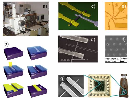
For the creation of pre-designed nanostructures the electron-beam lithography (EBL) is the most effective method. We are operating an electron-beam lithography system (a) in collaboration with MFA (Research Institute for Technical Physics and Matherial Science), which is based on a Jeol 848 scanning electron microscope. The principle of EBL (b): a thin polymer layer is scanned by the electron beam. The irradiated regions can be removed by chemical processing, forming a mask for evaporation. Metal is evaporated on the mask, and the remainder of the PMMA is removed. With these steps complex metallic nanostructures can be produced down to range of 40-100 nm. We use the EBL system to fabricated electric circuits from different nanoscaled objects (e.g. semiconducting nanowires, graphene, carbon nanotubes). These objects are contacted with different type of electrodes (normal, superconducting, ferromagnetic), local gates are fabricated in their close vicinity, with the aim to define hybrid nanodevices demonstrating novel quantum behaviors.
|
|
|
a) E-beam lithography system based on a Jeol 848 Scanning Electron Microscope (SEM) b) Principle of electron beam lithography c)Design of a hybrid nanocircuit and SEM picture of its realization e) Graphene flake contacted in a Hall-geometry, f) Typical resolution of our E-beam lithography system: ~40nm holes in a 400nm thick PMMA, g) Fabricated nanocircuits are bounded in chip carriers and placed into sample holders in order to study their transport behavior at low temperature. |