![]()
Molecular electronics laboratory
![]()
|
|
Molecular electronics laboratory |
|
Molecular electronics, the application of single or a few molecules as active region of electronic devices, has been proposed for many years as an alternative of present semiconductor technologies. The realization of molecular electronics could lead to a considerable downscaling of the building blocks of electronic devices. Furthermore, taking advantage of the wide possibilities in the chemical design of molecular
structures, molecular electronics devices are promising candidates for novel atomic-scale memory elements or ultra-sensitive nanoscale sensor technologies. However, beside its rich perspectives the field of molecular electronics is hindered by several difficulties. Contrary to the well-controlled engineering of semiconductor circuits, molecular electronics highly relies on the self-organization of the molecules, and the fine details of the interaction with the contacting electrodes. Usually – due to their extremely small sizes – single molecule devices cannot be imaged directly, and all the information about the device is obtained from indirect electronic measurements. In many cases it is already very hard to answer the most fundamental question, whether really a single piece of the chosen molecule is contacted, and obtaining comprehensive knowledge about the precise conformation of the molecular nanostructure is almost impossible. Due to the above difficulties the development of reliable contacting technologies with a large number of control parameters is of utmost importance.
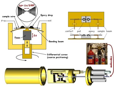
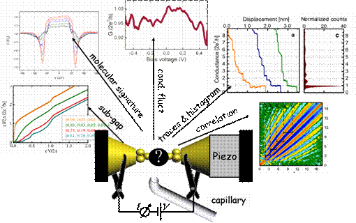
For the experiments we apply the idea of the mechanically controllable break junction (MCBJ) technique. An atomic-sized contact is created by gently breaking a metallic wire which is fixed on the top of a flexible substrate with two drops of epoxy. The wire is broken by bending the substrate in a 3 point bending configuration. The coarse positioning is performed by a screw thread mechanism, whereas for fine tuning a piezo actuator is applied. Due to the special mechanical arrangement of the setup the displacement of the electrodes is reduced by two orders of magnitude with respect to the elongation of the piezo. This high transmission ratio, the rigid construction of the sample holder, the cryogenic circumstances and the vibrational isolation of the research dewars lead to an extreme mechanical stability on the picometer scale. The experiments are performed by self-designed low-temperature MCBJ setups. The molecules are dosed to the junction in-situ through a heated capillary tube. In the cryogenic vacuum the cleanliness of the freshly broken contacting surfaces can be guarantied for a long time, therefore a large variety of materials can be applied as electrodes including the strongly reactive metals.
|
|
|
The principle of MCBJ technique (top left), the sample (top right) and the design of the sample holder (bottom) |
The MCBJ setup enables a large variety of measurements:
|
|
|
Several measurement methods are available with the MCBJ technique. |
· We have pointed out the importance of the electrodes contacting the molecules by showing that the change in the local density of states of palladium contacts due to the dissolution of hydrogen strongly influences the conductance of the molecular structure [1].
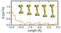
· We have demonstrated that gold, well-known from its inertness on its macroscopic surfaces is highly reactive on nanoscale. According to our results a hydrogen molecule can be incorporated in the gold nanocontact, and this hydrogen clamp is strong enough to pull a chain of gold atoms [2].
|
|
A chain of gold atoms is pulled with a hydrogen clamp, which is reflected by a periodic structure in the conductance trace. |
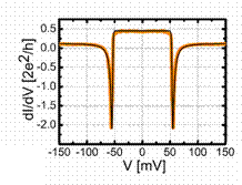
· We have shown that I-V characteristics of molecular nanojunctions frequently show huge nonlinearities, even negative differential conductance due to the excitation of a strongly bound molecule to a large number of energetically similar loosely bound states [3].
|
|
Huge negative differential conductance phenomenon in the dI/dV curve of a Au-H2 nanojunction |
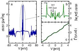
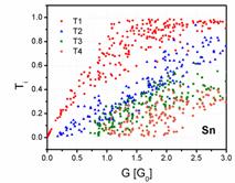
· We have investigated the opening of conductance channels in atomic and molecular contacts by superconducting subgap method. Subgap structure measurements give a unique opportunity for the full determination of transmission probabilities for all the conductance channels, and the evolition of the channel transmission as a function of total conductance is characteristic of the studied system, providing significantly more information than the conductance histogram alone [4]
|
|
|
|
I-V curve measurement on a superconducting molecular nanojunction (left). In the gap region distinct structures are observed at the fractional values of the gap due to multiple Andreev reflections. By fitting the I-V curve the number of open channels and the individual transmission probabilities can be determined. The evolution of the individual transmission probabilities as a function of total conductance (right) is characteristic of the studied material. |
|
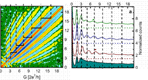
· We have developed a novel statistical method based on the cross-correlation analysis of conductance traces. This method is capable of resolving several features of nanocontact formation dynamics, which are completely hidden in traditional conductance histograms, including the correlated and anticorrelated occurrence of different junction configurations, and the resolution of fine structures which are obscured in the histogram by random variations of the conductance. We have discovered robust structures in the correlation diagrams of Ni, Fe and V contacts, which demonstrate a very regular atomic narrowing of the junction, in contrast to the rather unordered rupture of Au nanowires [5].
|
|
|
Robust stripes in the cross-correlation plot and numerous peaks in the conditional histograms of Ni contacts indicate a very regular atom by atom narrowing of the nanojunction. |
[1] Sz. Csonka, A. Halbrititer, G. Mihály, O.I. Shklyarevskii, S. Speller, and H. van Kempen, Conductance of Pd-H nanojunctions, Phys. Rev. Lett. 93, 016802 (2004).
[2] Sz. Csonka, A. Halbritter, and G. Mihály, Pulling gold nanowires with a hydrogen clamp: Strong interactions of hydrogen molecules with gold nanojunctions, Phys. Rev. B 73, 075405 (2006)
[3] A. Halbritter, P. Makk, Sz. Csonka, and G. Mihály, Huge negative differential conductance in Au-H2 molecular nanojunctions, Phys. Rev. B 77, 075402 (2008)
[4] P. Makk, Sz. Csonka, A. Halbritter, Effect of hydrogen molecules on the electronic transport through atomic-sized metallic junctions in the superconducting state. Phys. Rev. B. 78, 045414 (2008).
[5] A. Halbritter, P. Makk, Sz. Mackowiak, Sz. Csonka, M. Wawrzyniak, J. Martinek, Atom by atom narrowing of transition metal nanowires resolved by 2D correlation analysis. arXiv:1006.1811v1